Philips BGW200 Design Page
 Philips has an interesting chip called the BGW200 that allows 802.11b connectivity with a SPI and/or SDIO interface. Unfortunately they are very tight about releasing any information on how to design with it. I did some work with this device and had some success in designing a board and interfacing to it. I never completed the whole project because I found a better way to provide 802.11 connectivity using alternative devices.
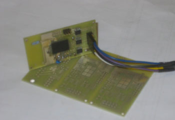
Included in this page is some of my work and documentation that should be useful to anyone who wishes to use this device. I have a working schematic and board layout, and was successful in interfacing to it via SPI using an Atmel controller. One of the first hurdles you will find in designing around the BGW200 is that the oscillator circuit is done in a non-standard way compared to most designs. Without this information it is very hard to get the BGW200 to startup and have a clock. Philips release a data sheet for the device describing the pins and software interface, but it is nowhere complete. This specification sheet neglected to describe the clocking and the software interface only described the interface registers and not what they did. Using my schematic you should be able to build a working board. I've also designed a 2-layer PCB board with express PCB that is a useful starting place for any design.
As for software to driver the BGW200 this also presents a problem, I was lucky enough to receive a ADYA system development board and software package that could be utilized to attach an ARM7 to the device. At first glance it did not contain the source code for the BGW200 driver only the object form. But after further investigation it contained the .lst files for the drivers that did contain the source code, it just needed to be extracted. I wrote a simple program to extract the source code. With this I was able to port it to the AVR processor.
One of the things I first found is that the BGW200 required firmware and that it was around 127Kbytes. This had to be loaded via the SPI interface from the processor or loaded via a serial EEPROM. The board I designed supports both. Some of the bigger AVR processors have enough flash to contain this firmware, most don't. Though booting from EEPROM is also not very well documented.
There is much more in my notes, but that can be for another day, the hardware design follows below.
Pictures
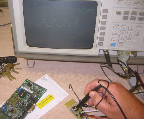
Clock Picture BGW200 with clock (and ADYA systemes board shown on the side).
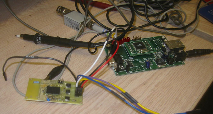
AVR dev board + BGW200 picture.
Design Documents
PDF schematic of my BGW200 board design.
Express PCB schematic of my BGW200 board design.(soon)
Express PCB board layout of my BGW200 board design.(soon)
Spec Documents
BGW200 Spec Sheet Useful but not complete. (soon)
Related Links
| 